
In the realm of PCB (Printed Circuit Board) and PCBA manufacturing, precision and reliability are paramount. As electronic devices become more sophisticated, so too must the methods used to ensure the highest quality of their components. One of the most effective and flexible methods for testing PCBs during manufacturing is Flying Probe Testing.
This innovative testing technique is critical for quality control, especially in prototypes, small to medium-volume production runs, and complex circuit designs. In this article, we’ll explore how flying probe testing works, its benefits, its applications, and why it has become an indispensable part of the PCB manufacturing process.
What is Flying Probe Testing?
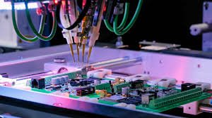
Flying probe testing is a non-contact electrical testing method used in PCB manufacturing to inspect electrical connections and verify the functionality of the circuit board. Unlike traditional testing methods, which rely on custom test fixtures or bed-of-nails setups, flying probe testers use mechanized probes that “fly” across the PCB’s surface to test individual points.
The system works by using a series of probes controlled by a robotic arm to contact specific points on the PCB. These probes check for faults such as short circuits, open circuits, improper component placement, and component orientation. The versatility of flying probe testing makes it ideal for low-to-medium-volume production and prototype testing, where custom fixtures are often not cost-effective.
How Does Flying Probe Testing Work?
The process of flying probe testing is efficient and highly automated, consisting of several key steps:
- PCB Loading and Setup: The PCB is loaded into the test machine. The flying probe system uses the Gerber file or PCB design data to map out the test points. These files define the locations where probes will make contact with the board.
- Movement of Probes: Once the PCB is placed, the robotic arm with multiple electrical probes moves across the surface of the board. The probes make contact with predefined test points, which are typically the pins of components, pads, vias, and traces on the PCB.
- Electrical Testing: During the testing phase, the system checks for:
- Continuity: Verifying that electrical paths are intact and not broken.
- Short circuits: Identifying unintended connections between different points.
- Open circuits: Detecting missing or improperly connected traces.
- Component placement and orientation: Ensuring that components are correctly placed and oriented according to the design specifications.
- Feedback and Error Detection: If any issues are detected, the system flags them and provides feedback to the operator. This feedback can include details about the type and location of the fault, allowing manufacturers to make corrections before proceeding with further assembly or shipping.
- Final Report: After testing is complete, the flying probe system generates a comprehensive test report, which outlines the results and identifies any faults found. This report is a valuable tool for ensuring that only high-quality, defect-free PCBs are shipped to customers.
Key Advantages of Flying Probe Testing
- No Need for Custom Fixtures
One of the most significant advantages of flying probe testing is that it doesn’t require custom-made test fixtures, which are typically necessary for traditional test methods like in-circuit testing (ICT). This makes flying probe testing more flexible and cost-effective, especially for small runs or prototypes where creating custom fixtures would be impractical.
3348. Fast Setup for Prototypes and Small Batches
Flying probe testing is particularly beneficial in environments that require fast turnaround times for prototypes or small to medium-volume production. Since it doesn’t require the setup of custom test fixtures, manufacturers can begin testing new designs more quickly, speeding up the time-to-market for new products.
3349. Highly Accurate and Precise
Flying probe testing is known for its accuracy and precision. The automated system can detect even the most minor faults, such as small shorts or improperly placed components. This high level of accuracy is especially important in industries where reliability is critical, such as in medical devices, automotive electronics, and aerospace.
3350. Versatility for Complex Designs
As PCB designs grow more intricate, especially in high-tech fields like telecommunications and advanced consumer electronics, traditional testing methods often struggle to keep up. Flying probe testing, however, is incredibly versatile and can test complex, multi-layer PCBs with ease. It is well-suited for fine-pitch components and high-density designs, which are increasingly common in modern electronic products.
3351. Cost-Effective for Low to Medium Volumes
Traditional testing methods, such as bed-of-nails testing, require expensive custom fixtures for each PCB design. These fixtures can be prohibitively expensive, especially for small-volume production runs. In contrast, flying probe testing eliminates the need for such fixtures, making it an affordable solution for low to medium-volume production and prototypes.
3352. Reduced Risk of Damage
Flying probe testing is non-invasive and doesn’t require physical contact with sensitive PCB components, reducing the risk of damage during testing. The system uses gentle probes that lightly touch the test points, ensuring that the PCB is not subjected to unnecessary stress or wear, making it ideal for fragile or delicate boards.
Applications of Flying Probe Testing
Flying probe testing is used across a wide range of industries that rely on high-quality PCB manufacturing. Some of the key applications include:
- Consumer Electronics: Testing for the assembly of smartphones, tablets, laptops, and other personal electronic devices.
- Medical Devices: Ensuring the functionality of PCBs used in critical medical applications like pacemakers, diagnostic machines, and patient monitoring systems.
- Automotive: Verifying the reliability of electronic components in vehicles, including control units, sensors, and infotainment systems.
- Aerospace and Defense: Testing high-performance PCBs used in satellite systems, radar, and communication equipment.
- Telecommunications: Ensuring that PCBs in telecom devices, including routers and base stations, meet quality standards.
Limitations of Flying Probe Testing
While flying probe testing offers numerous advantages, it does have some limitations:
- Slower for High-Volume Production
For very high-volume production runs, flying probe testing may not be as fast as other methods, such as in-circuit testing with custom fixtures. Since the probes test one point at a time, the process can take longer compared to parallel testing methods that can test multiple points simultaneously.
6817. Complexity with Large-Scale Boards
While flying probe testing can handle complex designs, it may struggle with large PCBs with numerous test points. Testing such boards can be time-consuming, and other methods may be more efficient for mass production of large, simple designs.
Conclusion
Flying probe testing has become an integral part of the PCB manufacturing process due to its flexibility, accuracy, and cost-effectiveness. It offers several benefits, particularly in low-to-medium volume production, prototype testing, and for complex, multi-layer boards. The ability to detect electrical faults early in the production process ensures that only high-quality boards are shipped, reducing the risk of product failures and enhancing customer satisfaction.
As electronics continue to evolve, and as designs become more intricate and demanding, flying probe testing will remain a valuable tool for ensuring that PCB manufacturers can maintain high standards of quality and reliability.


